Scientists twist tiny crystals to control electricity
- Date:
- January 25, 2026
- Source:
- RIKEN
- Summary:
- Researchers have developed a technique that allows them to carve complex three dimensional nanodevices directly from single crystals. To demonstrate its power, they sculpted microscopic helices from a magnetic material and found that the structures behave like switchable diodes. Electric current prefers one direction, but the effect can be flipped by changing the magnetization or the twist of the helix. The findings show that geometry itself can be used as a tool for electronic design.
- Share:
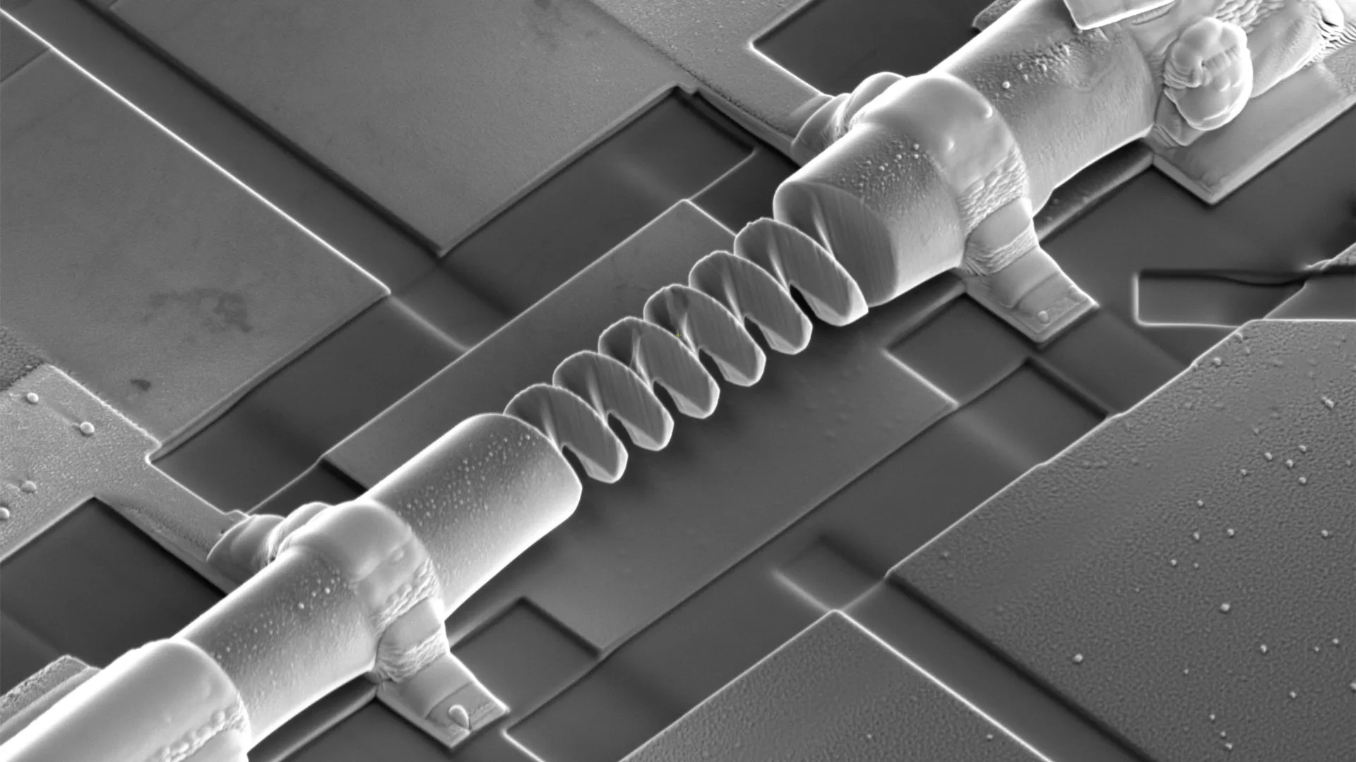
Scientists at the RIKEN Center for Emergent Matter Science, along with their collaborators, have developed a technique for building three dimensional nanoscale devices directly from single crystal materials. The method relies on a focused ion beam instrument that can precisely remove material at extremely small scales. Using this approach, the team carved tiny helical structures from a topological magnetic crystal made of cobalt, tin, and sulfur, with the chemical formula Co3Sn2S2. Tests showed that these structures behave like switchable diodes, meaning electric current travels more easily in one direction than the other.
Electronics built with complex three dimensional shapes could be smaller, more efficient, and more powerful than today's flat devices. Despite this potential, researchers have had limited ways to create such structures. Existing fabrication methods often restrict which materials can be used and can compromise the quality of the final device.
Precision Cutting With Focused Ion Beams
In the new study, published in Nature Nanotechnology, the researchers addressed these challenges by using a focused ion beam capable of cutting with sub micron precision. This level of control allows, in principle, the creation of three dimensional devices from nearly any crystalline material. The process resembles sculpting, where material is carefully removed from a solid block until the desired form is achieved.
To demonstrate the capabilities of the method, the team fabricated helical nanodevices from the magnetic crystal Co3Sn2S2. Based on the known properties of this material, they expected the twisted geometry to produce a special diode effect called nonreciprocal electrical transport, driven by the chiral shape at the nanoscale. Experiments confirmed this prediction. Electric current flowed more easily in one direction, and the effect could be reversed by changing the magnetization or switching the handedness of the helix. The researchers also observed the reverse interaction, where strong electrical pulses could flip the magnetization of the structure. Diodes are essential components in modern electronics and are used in AC/DC conversion, signal processing, and LED devices.
How Shape Controls Electron Motion
By comparing helices of different sizes and measuring their behavior at various temperatures, the researchers traced the diode effect to uneven scattering of electrons along the curved, chiral walls of the devices. These findings show that the physical shape of a component can directly influence how electricity moves through it. The results suggest that geometry itself can be used as a design tool, enabling low power, shape engineered components for future memory, logic, and sensing technologies.
According to Max Birch, the first author of the study, "By treating geometry as a source of symmetry breaking on equal footing with intrinsic material properties, we can engineer electrical nonreciprocity at the device level. Our newly developed focused ion beam nanosculpting method opens up a wide range of studies on how three dimensional and curved device geometries can be used to realize new electronic functions."
Yoshinori Tokura, who leads the research group, added, "More broadly, this approach enables device designs that combine topological or strongly correlated electronic states with engineered curvature in the ballistic or hydrodynamic transport regime. The convergence of materials physics and nanofabrication points to functional device architectures with potential impact on memory, logic, and sensing technologies."
Story Source:
Materials provided by RIKEN. Note: Content may be edited for style and length.
Journal Reference:
- Max T. Birch, Yukako Fujishiro, Ilya Belopolski, Masataka Mogi, Yi-Ling Chiew, Zhuolin Li, Xiuzhen Yu, Naoto Nagaosa, Minoru Kawamura, Yoshinori Tokura. Nanosculpted 3D helices of a magnetic Weyl semimetal with switchable non-reciprocal electron transport. Nature Nanotechnology, 2026; DOI: 10.1038/s41565-025-02104-x
Cite This Page: