New light trap design supercharges atom-thin semiconductors
Scientists turned empty space into powerful light traps—unlocking a huge boost for ultra-thin semiconductors.
- Date:
- March 24, 2026
- Source:
- SPIE--International Society for Optics and Photonics
- Summary:
- Scientists have found a clever way to supercharge ultra-thin semiconductors by reshaping the space beneath them rather than altering the material itself. By placing a single-atom-thick layer of tungsten disulfide over tiny air cavities carved into a crystal, they created miniature “light traps” that dramatically boost brightness and optical effects—up to 20 times stronger emission and 25 times stronger nonlinear signals. These hollow structures, called Mie voids, concentrate light exactly where the material sits, overcoming a major limitation of atomically thin devices.
- Share:
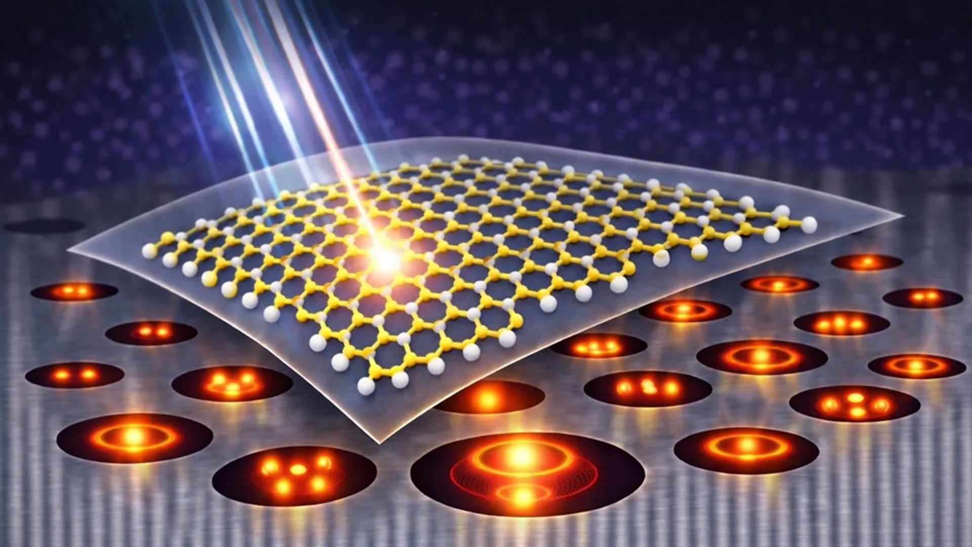
Atomically thin semiconductors like tungsten disulfide (WS2) are emerging as key materials for next-generation photonic technologies. Even though they are only a single layer of atoms, they can host tightly bound excitons, which are electron and hole pairs that interact strongly with light. These materials can also produce new colors of light through nonlinear optical effects such as second-harmonic generation. Because of these properties, they are promising for applications in quantum optics, sensing, and compact on-chip light sources. However, their extreme thinness also creates a challenge. With so little material available, light has limited interaction, which often results in weak emission and inefficient frequency conversion unless the surrounding photonic environment is carefully designed.
A study published in Advanced Photonics presents a new strategy to overcome this limitation by modifying not the material itself, but the space beneath it. In this approach, a single layer of WS2 is placed on nanoscale air cavities, called Mie voids, which are carved into a high-index crystal of bismuth telluride (Bi2Te3). These tiny voids significantly boost light emission and nonlinear optical signals. They also make it possible to directly observe localized optical modes, offering new insight into how light behaves at very small scales.
Turning Empty Space Into a Light Resonator
Traditional dielectric nanoresonators trap light inside solid materials like silicon. While effective in many cases, this design keeps the strongest optical fields away from the surface where atomically thin materials sit. It also becomes less efficient when the material absorbs light, which weakens the resonance and reduces field intensity.
Mie voids work differently. Instead of trapping light inside solid matter, they confine it within subwavelength air cavities etched into a material with a very high refractive index. Strong reflections at the air-dielectric boundary keep the light circulating inside the cavity. As a result, the optical field is concentrated in the air region and near the top surface, exactly where the WS2 layer is located.
This "inverted" confinement approach offers several benefits. The enhanced field is directly accessible to surface materials, the resonant wavelength can be tuned by adjusting the cavity shape, and the design remains effective even in materials that strongly absorb light. Bi2Te₃, which is not ideal for conventional resonators, performs well in this void-based configuration.
Designing and Building the Structure
Using detailed electromagnetic simulations, the researchers designed cavities that support a dipolar resonance aligned with the main emission feature of WS2, known as the A-exciton. By carefully adjusting the radius and depth of each cavity, they could control both the resonance wavelength and the vertical position of the optical mode.
The cavities were created using focused ion beam milling in thick, mechanically exfoliated Bi2Te3 flakes. They were spaced far enough apart to function as individual resonators rather than interacting with one another. A continuous WS2 monolayer was then transferred across the patterned surface, covering resonant cavities, non-resonant cavities, and flat regions. This design ensured that any differences in optical behavior were due to the cavity geometry and not variations in the material itself.
Optical reflection measurements confirmed that the cavities behaved as expected. Larger cavities caused a smooth shift of the resonance toward longer wavelengths, while changes in depth altered both the spectral position and the vertical location of the optical mode. Importantly, the resonances remained stable even when the geometry was not perfectly optimized, showing that the design is tolerant of fabrication imperfections.
Boosting Light Emission From WS2
To understand how the cavities affect light emission, the team measured photoluminescence from WS2 under laser excitation while varying the cavity depth. When the cavity resonance matched the WS2 emission band, the light output increased by about 20 times compared to the least resonant cavity.
Further analysis showed that this boost was not due to stronger absorption of the incoming light. Simulations indicated no significant enhancement at the excitation wavelength, and experiments using different pump wavelengths consistently produced the strongest emission at the same cavity depth. This confirms that the improvement comes from emission-related effects. The resonant cavity increases the local optical density of states and helps emitted light escape more efficiently.
Because the WS2 layer was continuous across the sample, researchers could directly compare emission from different regions under identical conditions. This demonstrated that the enhanced emission was driven by the engineered cavity modes rather than differences in the material itself.
Nonlinear Optics and Visualizing Light Modes
The team also explored nonlinear optical effects by adjusting the cavity geometry so that the resonance shifted into the near-infrared range. Under these conditions, the second-harmonic signal from WS2 increased by about 25 times compared to non-resonant cavities. The signal peaked when the excitation wavelength aligned with the cavity resonance.
In addition to boosting performance, the system allows direct visualization of optical modes. Far-field imaging of the second-harmonic signal revealed bright, localized hotspots above individual cavities. As the excitation wavelength or cavity depth changed, these hotspots moved in a predictable pattern across the array. This provided a clear, real-space view of how optical fields evolve inside individual resonators, without requiring specialized near-field techniques.
A New Platform for Atom-Thin Photonics
By combining adjustable optical enhancement with precise spatial control in a van der Waals-compatible system, Mie-void heterostructures offer a powerful new platform for working with atomically thin materials. Unlike traditional approaches, this method does not rely on large metasurfaces and remains effective even in materials that strongly absorb light.
This technology could enable advances in nonlinear light generation, surface-enhanced sensing, and programmable photonic devices based on two-dimensional semiconductors. More broadly, it shows that shaping empty space can be just as important as selecting the right material when designing nanoscale light-matter interactions.
Story Source:
Materials provided by SPIE--International Society for Optics and Photonics. Note: Content may be edited for style and length.
Journal Reference:
- Zhuoyuan Lu, Kirill Koshelev, Pavel Tonkaev, Ziyu Chen, Dawei Liu, Wenkai Yang, Yuri Kivshar, Yuerui Lu. Light–matter interaction in van der Waals heterostructures with Mie voids. Advanced Photonics, 2026; 8 (02) DOI: 10.1117/1.AP.8.2.026002
Cite This Page: